Introduction
The idea of the following text is to give a short
introduction to the topic of nanoscience and nano technology,giving an
access to more detailed texts.
As a short introduction to the above topics especially in the field of
semiconductor physics, we provide a short movie in high(77MB) and low(18MB) quality (sorry,
only in german).
A nanometer (nm) is one billionth of a meter or
10-9 meter. The relation between nanostructures and the
size of a football is the same as between the football and the
earth. Nanotechnology is the fabrication of materials or systems,
where at least one dimension is in the range of 1-100nm. By
manipulating matter at this length scale one hopes to achieve superior
electrical, chemical, mechanical and optical properties of these
material for applications in our macroscoic world.
In principle there are two different methods to
produce nanostructures:
Top Down
|
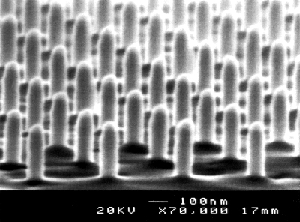
The most common way to fabricate structures in the
range of nanometers it the top-down approach. By using lithographic
processes the small nanostructured elements are "cut" from larger
pieces. The best known example is microelectronics.Today using optical
lithography semiconductor chips with critical dimensions down to 65nm
can be produced. Because of the limited resolution due to the
wavelength of the light already now special tricks have to be used
(such as phase shift masks). To realize structures in the range of 1nm
electron beam lithography is used.
|
|
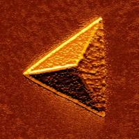
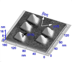
Bottom Up
|
The bottom-up approach utilizes methods of
selforganization on molecular and nanocrystalline levels. The most
impressive examples can be found in biology, e.g. the replication of
DNA strands or the selforganization of proteins.
The principle of
selforganization is not resticted to biological systems, but it can be
used in principle in arbitrary atomic or molecular systems, e.g. for
the synthesis of nanocrystalline materials and selforganized
semiconductor nanostructures.
|
|
|
In an optical microscope the size of the smallest
visible structure is in the range of the wavelength of the light (due
to it wave properties). Therefore nanostructures are not visivle in
optical microscopes.
There are several different methods to
characterize Nanostructures, some of them will be presented here.
In a Transmission Electron Microscope (TEM) electron beams are used
for imaging. Single atomic rows can be made visible and distances
belwox 0.1nm can be measured.
In a Scanning Tunneling Microscope (STM) or Atomic Force Miocroscope
(AFM) a sharp tip is scanned over the surface. In an STM a current is
measured, in an AFM the force between tip and sample surface (van der
Waals force). With both microscopes single atoms can be made visible.
|
|
Nanotechnology makes it possible to fabricate
smaller, faster computer chops for more efficient computers, mobile
phones or navigation systems.
It leads to new lasers like the quantum dot laser which enable faster
communication an new powerful data storage systems. The quantum
computer is a goal physicists all over the world are working on.
But nanotechnology does not only bring imrovements in the area of
semiconductor technology and microelectronics. The mastery of
materials and systems on the nanometer scale will also revolutionize
traditional areas. Nanostructured metallic and ceramic materials are
more buoyant, stronger and more rugged. Carbon nanotubes are more
elastic and robust than steel. Polymeres mechanically strengthened
with carbon nanotubes are used in areas from medicine to
aviation. Nanostructured surfaces are efficinet catalysts. They are
used in chemical engineering and in environmental sector.
One of the most interesting areas is the combinatio of nanotechnology
and biology. Scientists work with the methods of physics on a
molecular level, e.g. on DNA strands or on living cells, so that
single functionalities can be investigated, such as the interaction
between an cell and a pathogenic germ. Diseases can be diagnosed more
easily and custom made drugs can be developed hidering the pathogen to
attack the cell, while showing no side effects.
|