STARTSEITE
News (german)
What is Nanotechnology?
Studies
Nano in Linz
Nanoproject NSI
SRP IRoN
Gallery
Publications
Links
Contact
Impressum
|
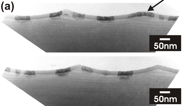
TEM images of annealed Si wires that were in situ covered with Ge.
(a) The darker part indicate areas, where holes in the oxide layer have formed
and the deposited Ge is polycristalline.
(b) High resolution TEM image: The holes in the SiO2 are decorated
with polycristalline Ge (p-Ge), which appears darker
than the amorphous Ge (a-Ge).
-
"Transient-enhanced Si diffusion on native-oxide-covered Si(001) nanostructure
s during vacuum annealing"
H. Lichtenberger, M. Mühlberger, F. Schäffler
Appl. Phys. Lett. 82 (21) 3650 (2003)
|
|